

Sustained high-bandwidth write workloads across modern PCIe 4.0 and PCIe 5.0 solid-state drives frequently trigger abrupt throughput degradation, plunging linear transfer speeds from 7,000 MB/s down to sub-SATA thresholds below 250 MB/s. When storage systems exhibit catastrophic performance drops during massive disk writes, database indexing, or local LLM model weights extraction, systems engineers must determine the physical root cause: is the drive experiencing silicon-level NVMe SSD thermal throttling at the controller junction, or has the flash translation layer (FTL) fully exhausted its dynamic pseudo-SLC cache allocation? Misdiagnosing this behavioral difference leads to misguided hardware modifications, ineffective cooler swaps, and persistent latency spikes across enterprise and workstation storage arrays.
Controller Junction Temperatures vs NAND Flash Thermal Physics
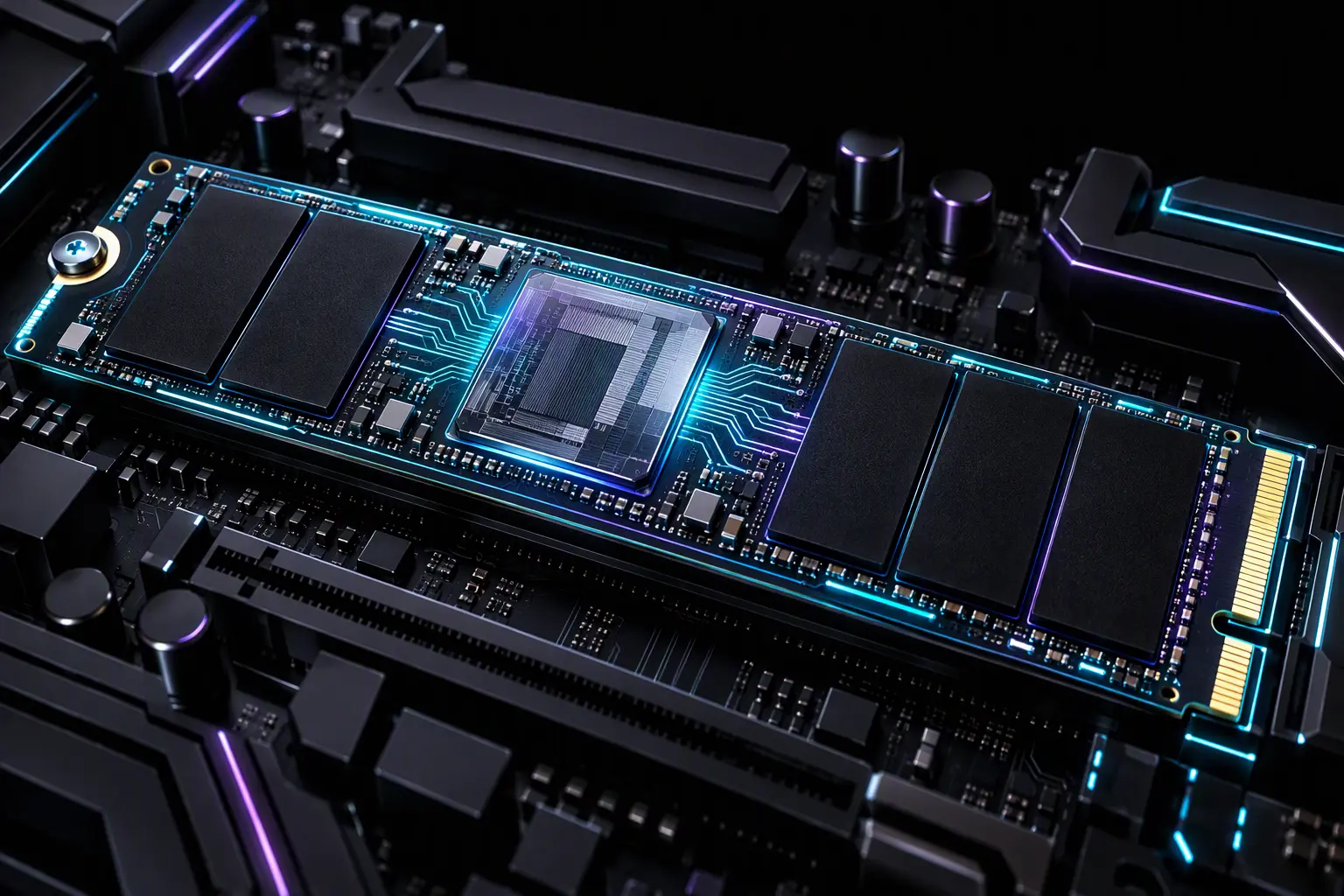
Modern solid-state architecture separates storage media into two physically distinct components with diametrically opposed thermal operational requirements: the high-speed controller ASIC and the multi-layer 3D NAND flash dies. High-performance controllers—such as the Phison PS5018-E18, PS5026-E26, and proprietary multi-core silicon from Samsung and Silicon Motion—function as miniature multi-core processors running complex algorithms for wear leveling, garbage collection, and direct memory access (DMA).
The controller ASIC generates high thermal density across an extremely compact die package (<100 mm²). When the controller junction temperature (Tj) reaches internal thermal threshold triggers—typically set between 80°C and 85°C according to the official NVM Express specifications—the drive initiates Thermal Management (TMT1/TMT2) routines. The controller reduces clock frequencies, introduces PCIe link state throttling, and inserts wait states into command processing queues to prevent thermal runaway.
Conversely, 3D TLC and QLC NAND flash memory cells exhibit superior data endurance and lower write wear when operating at warm ambient temperatures (ideally between 40°C and 60°C). Heating during program/erase (P/E) cycles lowers the electric field intensity required to tunnel electrons through the silicon dioxide dielectric layer, minimizing structural crystal degradation. When aggressive passive cooling or misconfigured custom water-blocks overcool NAND flash below 25°C while leaving the adjacent controller uncooled, raw bit error rates (RBER) escalate rapidly, increasing background ECC correction overhead.
NVMe SSD Thermal Throttling vs Dynamic SLC Cache Exhaustion
Differentiating between silicon thermal throttling and SLC cache exhaustion requires analyzing real-time input/output telemetry. Although both phenomena exhibit severe throughput collapse, their performance profiles and hardware metrics operate on distinct physical axes.
| Diagnostic Dimension | NVMe SSD Thermal Throttling (ASIC Junction) | SLC Cache Exhaustion (NAND Direct-to-Die) |
|---|---|---|
| Throughput Profile | Aggressive “sawtooth” waveform; cyclic throttling and recovery intervals. | Abrupt single-step cliff drop followed by an entirely flat low-speed plateau. |
| Primary Sensor Metric | HWiNFO64 Drive Temperature 2/3 (ASIC Hotspot) exceeding 80°C–85°C. | Drive temperatures remain stable (50°C–65°C); high controller queue utilization. |
| I/O Latency Signature | Erratic millisecond spikes across all queue depths (QD1 through QD64). | Consistent write latency elevation driven by real-time TLC/QLC cell folding. |
| Recovery Condition | Immediate recovery once airflow drops die temperature below hysteresis threshold. | Requires prolonged idle time for FTL garbage collection and TRIM processing. |
Unlike persistent NVMe SSD thermal throttling, which recovers quickly once temperatures drop below trip points, SLC cache exhaustion presents a prolonged performance penalty. On consumer DRAM-less solid-state drives utilizing Host Memory Buffer (HMB) architectures, the penalty is severe. Once the dynamic SLC allocation (which consumes three times the physical capacity on TLC drives) is depleted, the controller must simultaneously read existing SLC blocks, fold data directly into native TLC blocks, and commit incoming host writes. This saturation reduces write speeds down to 150–300 MB/s without thermal trip points ever triggering.
For more architectural comparisons on solid-state bus configurations, review our dedicated engineering analysis in Storage & RAM systems.
SMART Telemetry Extraction via PowerShell and NVMe-CLI
To isolate active NVMe SSD thermal throttling events without third-party monitoring overlays, query the hardware telemetry logs via the host operating system shell.
On Windows workstations and Windows Server environments, query the physical storage subsystem reliability counters directly through administrative PowerShell:
Get-PhysicalDisk | Where-Object { $_.BusType -eq "NVMe" } | Get-StorageReliabilityCounter | Format-List DeviceId, Temperature, TemperatureMax, WearTo inspect internal hardware temperature transition counts and evaluate whether the ASIC has crossed critical thresholds, extract the full hardware error log using the system storage driver diagnostics:
# Query NVMe-specific thermal transition history in Windows
Get-WmiObject -Namespace root\wmi -Class MSStorageDriver_ATAPISmartData | Select-Object -ExpandProperty VendorSpecific
On Linux-based hypervisors, NAS systems, and WSL2 environments, the industry-standard nvme-cli utility provides granular controller junction data:
# Install nvme-cli and read comprehensive smart-log telemetry
sudo apt install nvme-cli -y
sudo nvme smart-log /dev/nvme0n1 | grep -E "temperature|Warning|Critical|Thermal"
Inspect the output specifically for Thermal Management Temp 1 Transition Count and Thermal Management Temp 2 Transition Count. If these counters increment continuously during write-intensive tasks, thermal throttling is officially confirmed at the hardware layer.
Engineering Solutions: Heatsink Mounting and Thermal Pad Tolerances
Preventing hardware-induced NVMe SSD thermal throttling requires strict attention to physical thermal interface materials (TIM). Generic motherboard heatsinks often introduce mechanical clearance issues that compromise controller contact:
- Thermal Pad Thickness & Compression: Most M.2 controller packages sit at a slightly lower mechanical height (z-height) than adjacent NAND flash packages. Installing a uniform 1.0 mm thermal pad across the entire PCB frequently prevents the heatsink from applying sufficient clamping pressure to the controller ASIC. Utilize a 1.5 mm high-density silicone or phase-change pad over the controller, paired with a 1.0 mm or 0.5 mm pad over the NAND dies.
- PCB Bowing Prevention: Excessive clamping force from double-sided aluminum brackets can flex the multi-layer printed circuit board, fracturing micro solder balls under the BGA package. Always confirm that thermal pads compress by approximately 25% to 30% of their resting thickness without bowing the PCB substrate.
- Active Airflow Requirements for PCIe 5.0: Gen 5 drives drawing between 10W and 14W under load cannot maintain full throughput with passive motherboard heatsinks in sealed chassis. A minimum airflow velocity of 1.5 to 2.0 CFM across the heatsink fins is required to dissipate concentrated heat away from high-speed controllers.
Frequently Asked Questions
Does severe NVMe SSD thermal throttling permanently damage hardware?
No. Internal thermal throttling mechanisms (TMT1 and TMT2) are fail-safe thermal protections engineered into the NVMe controller firmware to prevent silicon degradation. When temperatures cross 80°C–85°C, clock speeds drop to keep the chip within safe operating junction temperatures. However, operating at continuous maximum thermal trip points accelerates long-term solder fatigue and compromises NAND cell charge retention over multi-year operational cycles.
Why do hardware monitors report multiple, conflicting SSD temperatures?
Modern NVMe drives expose several onboard thermal diodes. “Temperature 1” (Composite Temperature) represents a smoothed algorithmic composite reported for general OS power states. “Temperature 2” or “Temperature 3” typically reports the raw junction temperature (Tj) located directly beneath the controller silicon die. The controller junction frequently runs 15°C to 25°C hotter than the surrounding NAND flash packages.
Can SSD firmware updates resolve persistent NVMe SSD thermal throttling?
Firmware updates cannot alter basic thermodynamics or compensate for missing physical heatsinks, but manufacturers regularly release firmware updates to optimize dynamic thermal throttling curves. Optimized algorithms introduce progressive, stepped clock scaling rather than abrupt, catastrophic speed drops, stabilizing transfer rates during burst workloads.
For homelabs, remote testing, and staging environments, we run NVMe VDS instances on Erahost. Fast provisioning, European routing, and predictable I/O.
View NVMe Plans →